
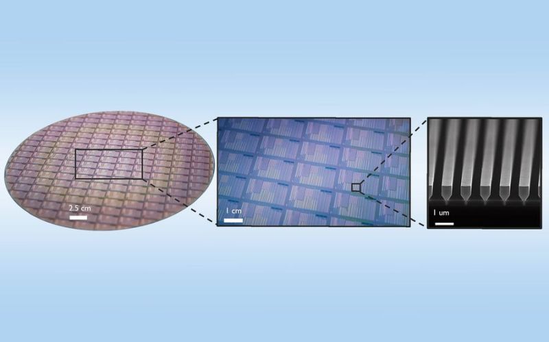
As great as silicon is for semiconductor applications, it has one weakness in that using it for lasers isn’t very practical. Never say never though, as it turns out that you can now grow lasers directly on the silicon material. The most optimal material for solid-state lasers in photonics is gallium-arsenide (GaAs), but due to the misalignment of the crystal lattice between the compound (group III-V) semiconductor and silicon (IV) generally separate dies would be produced and (very carefully) aligned or grafted onto the silicon die.
Naturally, it’s far easier and cheaper if a GaAs laser can be grown directly on the silicon die, which is what researchers from IMEC now have done (preprint). Using standard processes and materials, GaAs lasers were grown on industry-standard 300 mm silicon wafers. The trick was to accept the lattice mismatch and instead focus on confining the resulting flaws through a layer of silicon dioxide on top of the wafer. In this layer trenches are created (see top image), which means that when the GaAs is deposited it only contacts the Si inside these grooves, thus limiting the effect of the mismatch and confining it to within these trenches.
There are still a few issues to resolve before this technique can be prepared for mass-production, of course. The produced lasers work at 1,020 nm, which is a shorter wavelength than typically used, and there still some durability issues due to the manufacturing process that have to be addressed.
This articles is written by : Fady Askharoun Samy Askharoun
All Rights Reserved to Amznusa www.amznusa.com
Why Amznusa?
AMZNUSA is a dynamic website that focuses on three primary categories: Technology, e-commerce and cryptocurrency news. It provides users with the latest updates and insights into online retail trends and the rapidly evolving world of digital currencies, helping visitors stay informed about both markets.
